
Product laser
Products
Excellent material compatibility supports quartz, borosilicate, soda-lime, aluminosilicate, and other specialty glass types
Flexible patterning capabilities enable fabrication of round holes, square holes, blind vias, through vias, and micro-grooves as required
Outstanding deep-hole processing with aspect ratio up to 1:100, minimum hole diameter ≤ 5 μm
Good hole quality with smooth inner-side walls that are free of cracks and burs
High throughput and capacity optimized for large-scale production
Precise positioning and repeatability for micro-level accuracy
|
Specification |
Details |
|
Substrate Size |
4 to 12-inch round or square wafers |
|
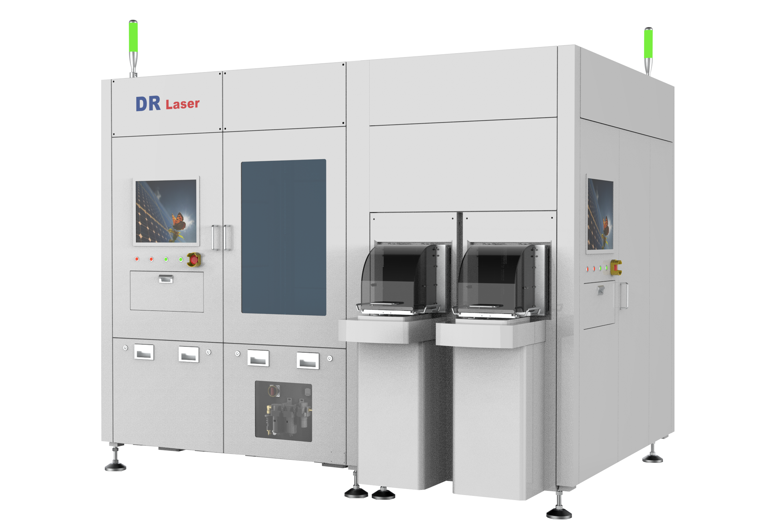
Loading Method |
Automated cassette feed (basket-type) for 4 to 12-inch wafers |
|
Processing Type |
Fixed-beam laser + high-precision motion platform |
|
Platform Speed |
≤ 1000 mm/s |
|
Hole Shapes |
Circular, square, blind via, through via, micro-trench |
|
Minimum Hole Diameter |
5 μm |
|
Maximum Aspect Ratio |
1:100 |
|
Platform Accuracy |
Repeatability ≤ ±1 μm; Positioning accuracy < ±2 μm |
|
Pattern Placement Accuracy |
≤ ±3 μm within a 300 mm processing range |
|
Throughput |
≥ 5000 points per second |

